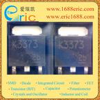
●最大源漏极电压Vds Drain-Source Voltage | 500V \---|--- 最大栅源极电压Vgs(±) Gate-Source Voltage | ±30V 最大漏极电流Id Drain Current | 2A 源漏极导通电阻ΩRds DΩ/Ohmain-SouΩ/Ohmce On-State Ω/Ohmesistance | 2.9Ω~3.2Ω(VGS =10V,ID= 1A) 开启电压Vgs(th) Gate-Source Threshold Voltage | Vth =2.0 to 4.0 V (VDS=10V,ID =1mA) 耗散功率Pd Power Dissipation | Description & Applications | TOSHIBA Field Effect Transistor Silicon N-Channel MOS Type (π-MOSV) . Switching Regulator and DC-DC Converter Applications. Motor Drive Applications .
● Low drain-source ON-resistance: RDS (ON)= 2.9 Ω (typ.)
● High forward transfer admittance: |Yfs| = 1.7 S (typ.)
● Low leakage current: IDSS = 100 μA (max) (VDS = 500 V)
● Enhancement model: Vth = 2.0 to 4.0 V (VDS = 10 V, ID = 1 mA) 描述与应用 | 东芝场效应晶体管的硅N沟道MOS型(π-MOSV)。 开关稳压器和DC-DC转换器应用。 电机驱动应用。
●低漏源导通电阻RDS(ON)=2.9Ω(典型值)
●较强的正向转移导纳:YFS| =1.7 S(典型值)
●低漏电流IDSS=100μA(最大值)(VDS=500 V)
●增强型号:VTH =2.0至4.0 V(VDS=10V,ID= 1毫安)